Novel Nanofabricated InP Photonic Integrated Circuits Devices
Published: 5 December 2024
Indium Phosphide (InP) is a crucial semiconductor material for photonic integrated circuits (PICs), yet its nanoscale fabrication is challenging. Xiao Sun presents several novel InP PIC devices with nanoscale fabrication achieved at JWNC.
Indium Phosphide (InP) is a crucial semiconductor material for photonic integrated circuits (PICs), yet its nanoscale fabrication is challenging. We present several novel InP PIC devices with nanoscale fabrication achieved at JWNC, realizing sub-100 nm fabrication in laser gratings, asymmetric waveguides, and photonic crystals, demonstrating world-class InP fabrication technology.
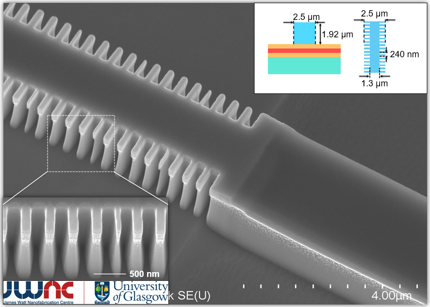
InP Nanoscale Sidewall Grating (fig 1)
Achieving smooth and vertical gratings is essential for sidewall DFB lasers. We present a fabrication recipe for InP grating waveguides with a grating period of 240 nm and a ridge height of 1.92 μm, yielding an aspect ratio of 1:8. The sidewall grating structure is applicable in semiconductor lasers, microcavity filters, and slow-light effect devices. Tools: E-beam lithography, ICP etching, and HSQ resist.
Asymmetric InP waveguide (fig 2)
Asymmetric waveguides are effective for optical mode conversion. We present a polarization mode converter utilizing a step-stage asymmetric waveguide, achieving a 98% conversion efficiency from TE to TM polarization. The primary application of these asymmetric waveguides lies in polarization mode modulation in free-space optical communication. Tools: E-beam, ICP etching and HSQ resist.
Topological photonic crystal based on InP (fig 3)
Photonic crystals (PhCs) have wide applications in lasers, slow-light effects, and nonlinear optics. We developed a process for fabricating 100 nm-scale 1550 nm valley-topological photonic crystals on InP. PC hole sizes range from 80-150 nm, with hole gaps as small as 35 nm. These structures are applicable in photonic crystal lasers and topological PhC waveguides. Tools: E-beam lithography, ICP etching, and PECVD.
Photonic crystal on ridge waveguide (fig 4)
We combined a dense PC array on ridge waveguides with depths of 3.5 μm and 3.3 μm. The PC holes have a 90 nm diameter and a 1.92 μm depth, yielding an aspect ratio of 1:21. These structures are applicable in photonic filters and multiplexers, lasers, and biosensors. Tools: E-beam lithography, ICP Cobra etching, and PECVD.
+++
Figure 1

---
+++
Figure 2

---
+++
Figure 3

---
+++
Figure 4

---
First published: 5 December 2024

