Superconducting Innovation at JWNC: Nb based Josephson Junctions for Quantum
Published: 21 January 2025
Wridhdhisom Karar, Jharna Paul (KNT), Valentino Seferai, Mohammed Alkhaledi, Kaivan Karami (KNT), David Milne (KNT), Martin Weides, Shimeng Xi.
State of the art fabrication aids in realizing quantum mechanics and unlocks quantum dynamics in macroscopic structures. Modern lithography has planarized resonance cavities in planar resonators of various materials, with quality factors exceeding machined 3D cavities, but the real innovation arose from observing quantum tunnelling effect in metal – insulator – metal junctions. Traditionally since the 90’s Aluminum based Josephson Junctions (JJs) have been easy to fabricate since the insulator(aluminum oxide) forms naturally.
The tunneling critical current of JJs are of the order of nA (nanoamperes) and their room temperate resistances are a order of a few kilo-ohms. This has been harnessed to produce quantum processing bits (qubits) but Aluminum has a superconducting temperature of 1.2K. Hence these qubits require millikelvin temperatures and has narrow, nanoampere supercurrent ranges.
An upgrade would be Niobium based JJs where the critical temperature is 9x of Al (9.3K) and critical tunneling currents would be of the order of microamperes ( times higher than Al) . These junctions have been realized in the structures in these images above. Deposition tools like Plassys VI is used to deposit a multilayered stack (Nb-Al-AlOx-Al-Nb) and further patterned into two overlapping electrode fingers. Dielectric spacers are used to prevent shorting electrodes and later removed using wet-etch techniques. After a series of runs, these devices have very low room temperature resistances of 100-1kOhms , and significantly high critical currents.
These junctions are presently incorporated into qubit-processing chips, and sensor based superconducting circuits for wide range of computing, and sensing applications.
+++
Figure 1
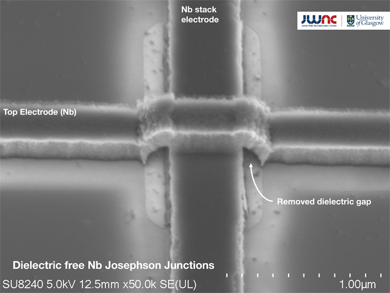
Novel dielectric free Niobium Josephson Junctions, prepared by removing a SiOx spacer using wet-etch methods.
---
+++
Figure 2
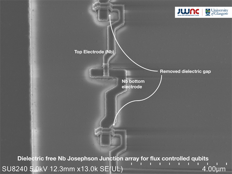
An array of such junctions can be controlled by applying magnetic flux to change the current flow through these junctions for quantum computing.
---
+++
Figure 3
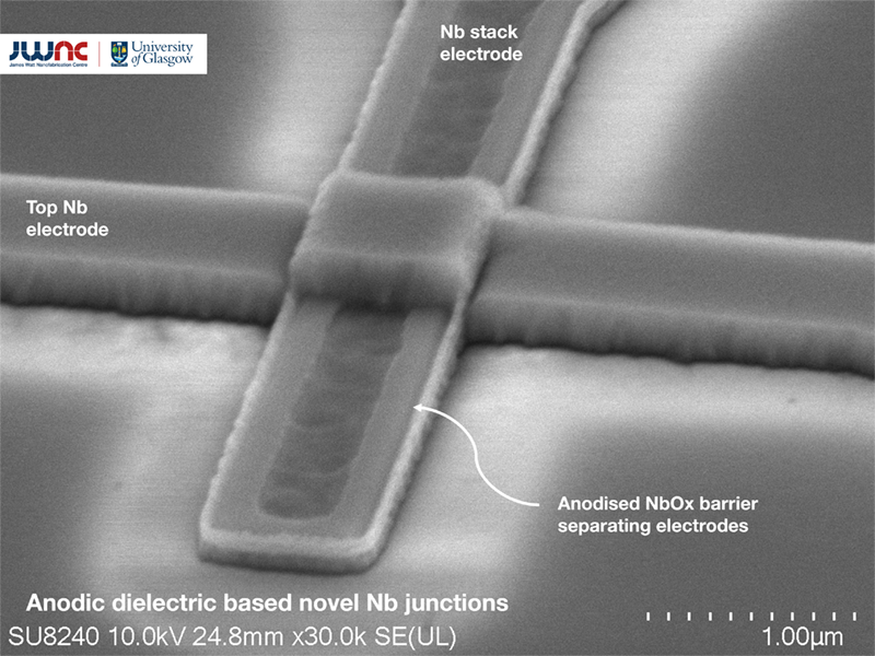
A different kind of anodic dielectric junctions with NbOx as a seperator between electrodes.
---
+++
Figure 4
---
+++
Figure 5
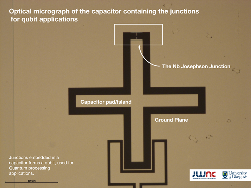
A qubit structure formed of a capacitor and a Nb junction shown. The junction typically is a few microns in size compared to the large capacitor it is embedded in. This electrically forms a qubit which a basis of Quantum Processing.
---
Quantum Circuits Group
The primary fabricators are Jharna Paul, Valentino and Kaivan Karami operating majority of the deposition, etching and process development with Wridhdhisom, Mohammed, Shimeng and David aiding with inspections, testing, measurement and characterisation of these devices. These devices are based on the designs by Wridhdhisom Karar. The group leader and project supervisor is Martin Weides.
Tools in JWNC:
- Plassys VI for deposition
- ICP180/300 for dry-etch
- PECVD Plasma Pro for SiOx spacers
- SU2480, Dektak Profiler, AFM for inspections
First published: 21 January 2025

