

Zeiss Sigma VP Analytical SEM with Oxford Microanalysis
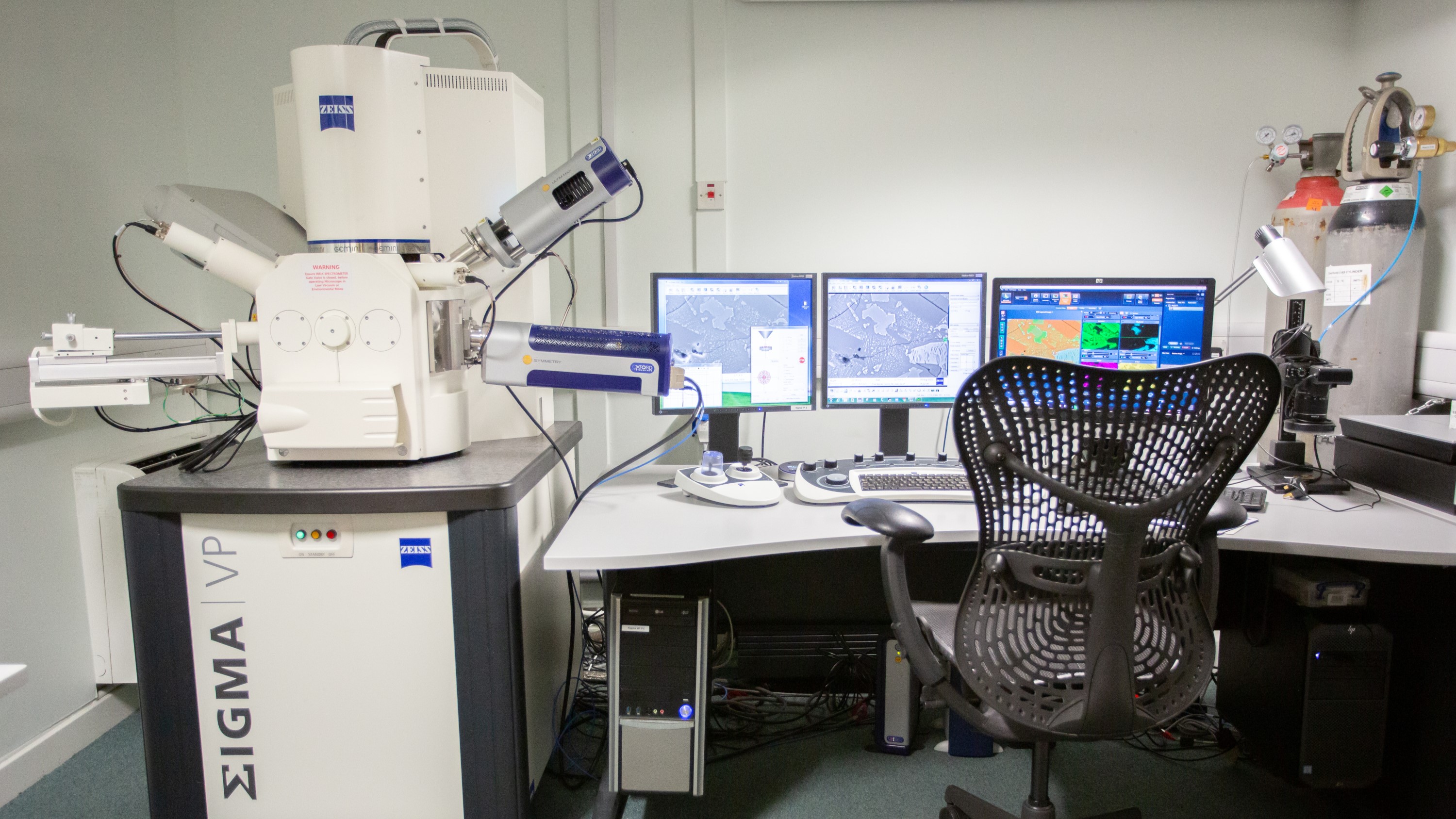
The Sigma is a field-emission SEM that produces exceptional images at high and low accelerating voltages. Together with its analytical capabilities, this instrument is suitable for a wide range of applications in materials and life science.
Sigma Capabilities:
- Electron source: Schottky thermal field emitter
- Accelerating voltage range: 0.2 to 30 kV
- Current range: 4 pA to 20 nA
- Variable pressure range: 2-133 Pa
- Detectors: In-lens secondary electron, Everhart-Thornley secondary electron, variable pressure secondary electron, backscattered electron, infra-red chamberscope
- Resolution at 1 kV/ 15 kV: 2.8 nm/1.5 nm
- Maximum image size: 3072 x 2304 pixels
- Large sample chamber that can accommodate specimens up to 250 mm diameter and 45 mm tall
Sigma Techniques:
- Secondary electron (SE), InLens and backscattered electron (BSE) imaging: all can be undertaken in high vacuum and low vacuum modes
- Energy-dispersive X-ray analysis (EDX): Oxford Instruments UltimMax Silicon Drift Detector (SDD) with 170 mm2 sensor size enables rapid determination of elemental compositions and acquisition of compositional maps
- Wavelength-dispersive X-ray analysis (WDX): Oxford Instruments WDX detector allows quantitative analysis and mapping of minor and trace elements that are below the detector limits for EDX detectors
- Electron backscatter diffraction (EBSD): the Symmetry 2 EBSD detector from Oxford Instruments allows determination of crystal structures and high-speed mapping of crystallographic orientations for crystalline materials at high spatial and angular resolution
- Cathodoluminescence (CL) imaging using VP SE detector allows acquisition of panchromatic CL imges across the visual spectrum
- Scanning Transmission Electron Microscopy (STEM): using a specialised detector from Zeiss, bright- and dark-field STEM images can be acquired from thin samples, enabling nano-scale imaging and elemental mapping
- Automated stage: motorized sample stage with sub-micron precision allows automated imaging, elemental and crystallographic mapping. This feature allows obtaining substantial data sets by mapping large areas of the sample at high resolution during nights and weekends without a presence of an operator