Vision
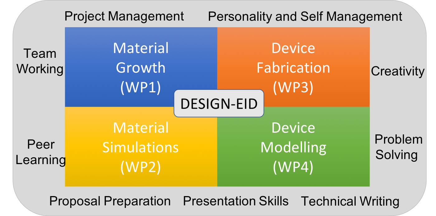
The mission of DESIGN-EID (Defect Simulations and Growth of III-V Nanostructures – European Industrial Doctorate) project is to train a pool of young Early Stage Researchers (ESR) in design, fabrication, characterisation and simulation of novel materials and device architectures with focus on material defects. This will be achieved by high quality and innovative research programs which will combine scientific (core) multidisciplinary training and transferable (soft) skills to our ESRs. DESIGN-EID unites an international and multidisciplinary network comprising 3 organizations – University of Glasgow (UK), IBM Research Zurich (Switzerland) and Synopsys QuantumATK (Denmark) in a targeted effort to create a training environment meeting the needs of the semiconductor and photonics industry. Our consortium will provide a unique research training opportunity and environment for a group of 3 young researchers in the novel, highly applicable and industrially relevant field of exploratory semiconductor materials and device development.
The three main objectives of the project are:
- Establishment of an industrially driven training network in advanced semiconductor materials development and simulation.
- Development of a simulation framework to capture the complexities of growth and defect formation in compound semiconductors.
- Experimental validation of modelling concepts via fabrication and characterisation of electronic and photonic III-V devices.

